Millions of viewers saw Sharna Burgess’ nip slip moment during the live television airing of Dancing with the Stars. She was dancing to the tune of tango with NFL star, Antonio Brown. Sharna Burgess’ wardrobe malfunction didn’t stop her from performing her best. She even revealed that she also had another wardrobe issue prior to that infamous moment, but she powered through.
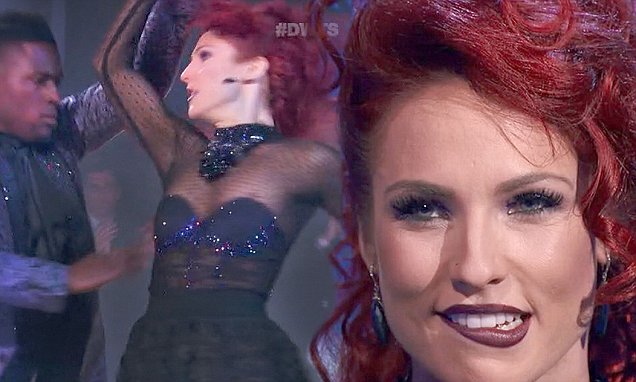
During a sexy tango performance, Sharna Burgess suffered from a nip slip, and it was caught on live television.

Despite what happened, she powered through with her performance and managed to impress the judges.
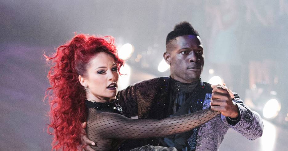
NFL star Antonio Brown was just as passionate as Sharna during their tango performance. Hence, none of them realized the nip slip moment.
Sharna is a dancing pro. Perhaps, the live nip slip wasn’t the first time that she suffered from wardrobe issue. Nevertheless, she had an amazing performance.
People were too obsessed with what happened on live TV, but they forgot that behind the drama, Sharna actually had an amazing performance.

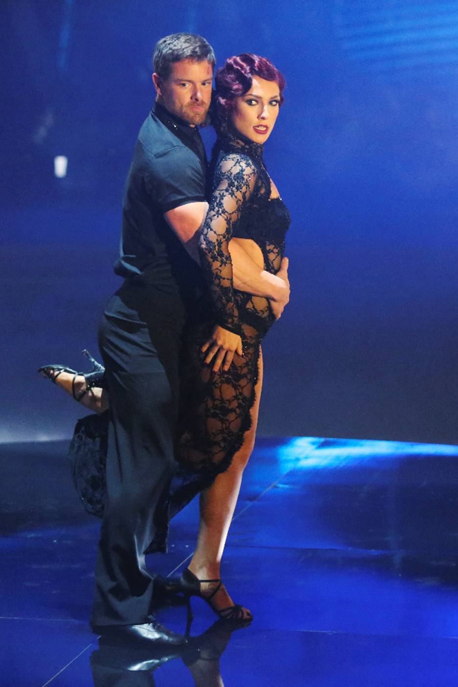
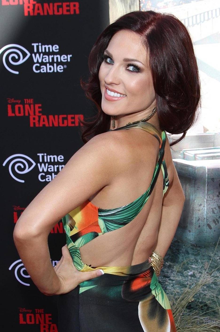
Sharna had been with Dancing with the Stars for quite a while and she has managed to impress the judges with her amazing skills.
Sharna said she would be more careful with her choices of clothing after what happened during that live performance.

Although the camera captured that infamous nip slip on live TV, it was actually not her first wardrobe issue of the night. She even had one earlier.

Sharna said that wardrobe malfunction can happen to anyone. She said that she learned a lot from the experience.
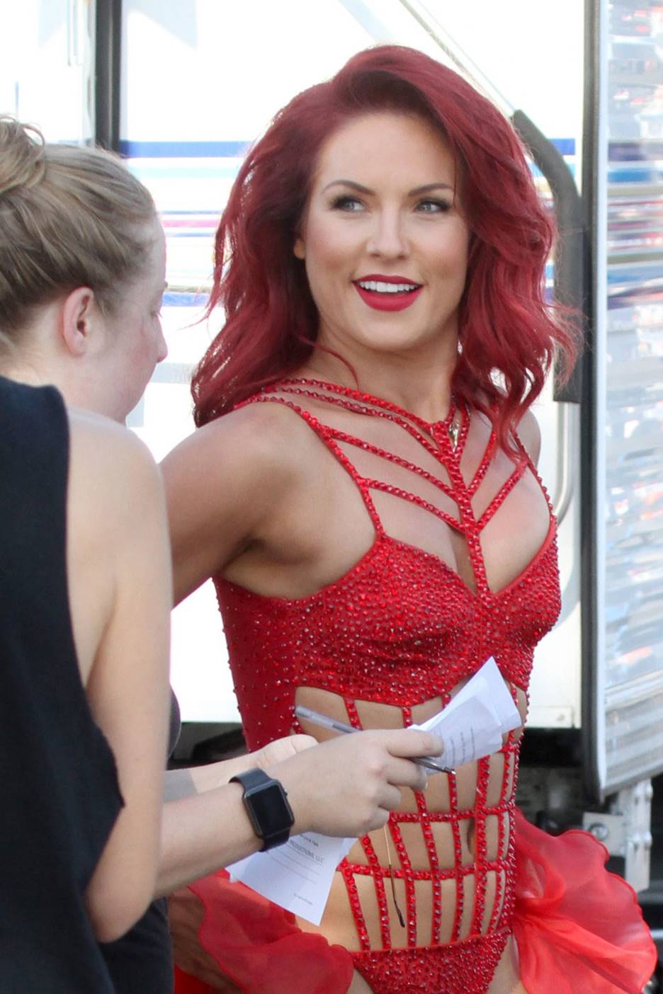
Despite what happened, she continued wearing sexy dancing clothes and has remained impressive in her on stage performances.